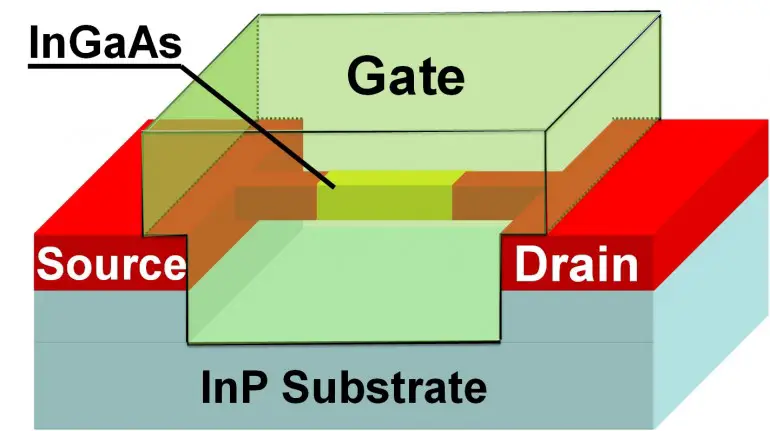
A transistor is the fundamental building block of all electronic devices. . A transistor can be defined as a device, which is used to amplify signals and power. Integrated circuits are used in making of chips inside electronic gadgets such as smart phones, laptops and so on. Researchers in Purdue and Harvard Universities have created a new type of transistor that will make the Integrated circuits more compact. This transistor is made from another material other than silicon and as the name suggest, a 3-D structure is given to the device compared to the conventional flat chips. Nano wires are used in these transistors instead of silicon so they will be more compact and more efficient. The nano wires used in this transistor are made from iridium gallium arsenide semiconductor.
Iridium-gallium-arsenide is replaced for silicon in this device. As they are elements from the 3rd and 5thgroup of the periodic table, they are collectively known as the III-V group semiconductors. These semiconductors are known to conduct electrons five times better than silicon. The mobility of this material is also known to be higher. All these characteristics have urged chip manufacturers to replace silicon with this semiconductor in the coming years.
The 3D transistor was made by a process termed ”top- down method” in which components of the transistor is etched. This method will gain huge acceptance as it is compatible with most of the industrial processes. In 2012, a new generation of integrated chips is believed to come into market in which transistors will be placed horizontally rather than vertically. This is the reason for the 3D effect posed by these transistors. Thus, this device is the world’s first 3D-gate-allround transistor.
The transistor consists of a gate by which rapid ON-OFF switching action is possible and helps in the direct flow of current. By the introduction of 3D transistors, it is estimated that this gate length will reduce from 45nm to 22 nm. The nano wires are coated with a dielectric, which acts as the gate. Further research is being conducted to reduce the gate length to 18 nm. The only option available is to make a thinner dielectric layer by a process called atomic deposition. A thinner dielectric layer offers greater speed, low voltage requirements and lower power consumption. The device has improved its clock speed to 20 GHz. This experiment was funded by the National Science foundation and Semiconductor research group. The latest development in this field was the design of a “finFET or fin Field Effect Transistor” in which the device has a fin like structure other than the conventional flat design.
By the introduction of 3D transistors computers will become faster, cooler and smarter. Intel is planning to release processors made from 3D transistor integrated chips in 2012. These chips are expected to be 10 times faster than the ones used now and will be more compact.
It is heard that a Japanese company named “Unisantis” is working with the researchers of Singapore’s Institute of micro electronics to develop a new 3D transistor called the SGT (Surrounding Gate Transistor) which will increase the clocking speed of the computers from 20 GHz to 50 GHz.
It is heard that a Japanese company named “Unisantis” is working with the researchers of Singapore’s Institute of micro electronics to develop a new 3D transistor called the SGT (Surrounding Gate Transistor) which will increase the clocking speed of the computers from 20 GHz to 50 GHz.


No comments:
Post a Comment